
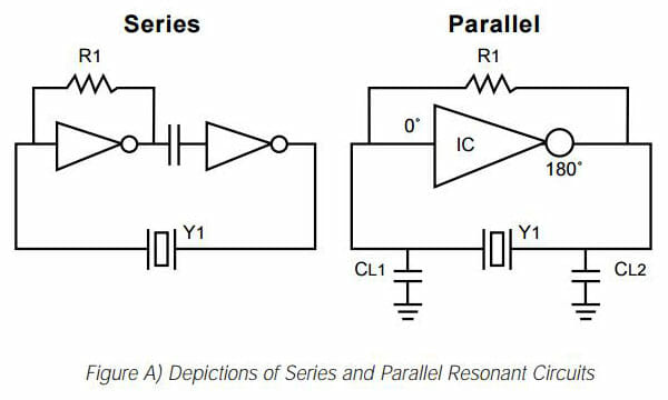
Series vs. Parallel: “Series” resonant crystals are intended for use in circuits which contain no reactive components in the oscillator feedback loop. “Parallel” resonant crystals are intended for use in circuits which contain reactive components (usually capacitors) in the oscillator feedback loop. Such circuits depend on the combination of the reactive components and the crystal to accomplish the phase shift necessary to start and maintain oscillation at the specific frequency. Basic depictions of two such circuits are shown below.
Load Capacitance: This refers to capacitance external to the crystal, contained within the feedback loop of the oscillator circuit. If the application requires a “parallel” resonant crystal, the value of load capacitance must be specified. If the application requires a “series” resonant crystal, load capacitance is not a factor and need not be specified. Load capacitance is the amount of capacitance measured or computed across the crystal terminals on the PCB.
Frequency Tolerance: Frequency tolerance refers to the allowable deviation from nominal, in parts per million (PPM), at a specific temperature, usually +25° C.
Aging: Aging refers to the cumulative change in frequency experienced by a crystal unit over time. The rate of frequency change is fasted during the first 45 days of operation. The most common factors affecting aging include drive level, internal contamination, crystal surface change, ambient temperature, wire fatigue and frictional wear. All of these problems can be minimized by proper circuit design which allows for low operating temperatures, minimum drive levels and static pre-aging.
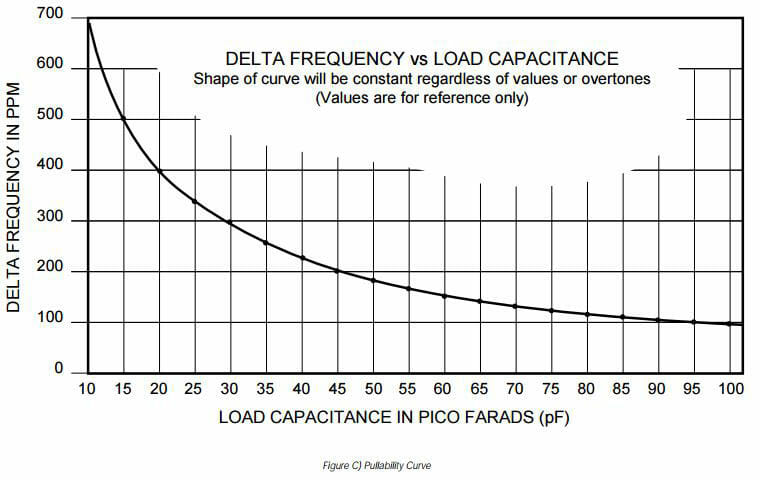
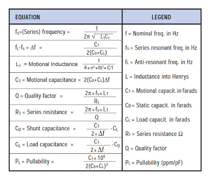
Pullability: Pullability refers to the change in frequency of a crystal unit, either from the natural resonant frequency (Fr) to a load resonant frequency (FL), or from one load resonant frequency to another. See Figure C. The amount of pullability exhibited by a given crystal unit at a given value of load capacitance is a function of the shunt capacitance (Co) and the motional capacitance (C1) of the crystal unit.
If pullability is a factor in design, collaboration with our engineers is advisable; bandwidth can be controlled to some extent, during fabrication, by varying the crystal parameters. An approximation of the pulling limits for standard crystals can be obtained from the following formula:
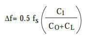
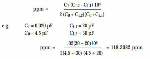
The exact limits also depend upon the Q of the crystal as well as associated stray capacitances. Pullability can be approximately doubled by modified crystal fabrication and by adding capacitance or inductance external to the crystal. If the Co and C1 are known then the pulling in ppm between two capacitances can be obtained using the following formula.
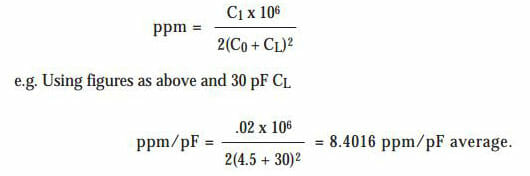
To obtain AVERGE pulling per pF about a known load capacitance use the following formula.
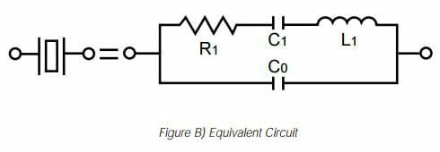
Equivalent Circuit: The equivalent circuit, shown in Figure B is an electrical depiction of the quartz crystal unit when operating at frequency of natural resonance. The CO, or shunt capacitance, represents the capacitance of the crystal electrodes plus the capacitance, of the holder leads. R1, C1 and L1 compose the “motion arm” of the crystal and are referred to as the motional parameters. The motional inductance (L1) represents the vibrating mass of the crystal unit. The motional capacitance (C1), represents the elasticity of the quartz and the resistance (R1), represents bulk losses occurring within the quartz.
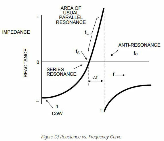
Impedance/Reactance Curve: A crystal has two frequencies of zero phase, as illustrated in Figure D. The first, or lower of the two, is Series Resonant Frequency, denoted as (ꬵs). At this point, the crystal appears resistive in the circuit, impedance is at a minimum and current flow is maximum. As the frequency is increased beyond the point of series resonance, the crystal appears inductive in the circuit. When the reactances of the motional inductance and shunt capacitance cancel, the crystal is at the Frequency of Anti-resonance, denoted as (fa). At this point, impedance is maximized and current flow is minimized.
Shock Characteristics: Although crystals are designed to handle normal shock in handling, shock impulses (such as half sine, square, sawtooth and complex combinations) can occur in the field. Because crystals are relatively delicate, they should be isolated from equipment to minimize shock damage. But, avoid over specification, since the elastic properties of the materials and the degree of isolation afforded by the equipment can decrease the destructive potential of a shock.
Quality factor (Q): The “Q” value of a crystal unit is a measure of the units relative quality, or efficiency of oscillation. The maximum attainable stability of a crystal unit is dependent on the “Q” value. In Figure D the separation between the series and parallel frequencies is called the bandwidth. The smaller the bandwidth, the higher the “Q” value, and the steeper the slope of the reactance. Changes in the reactance of external circuit components have less effect (less “pullability”) on a high “Q” crystal, therefore such a part is more stable.
Calculation of Load Capacitance: if the circuit configuration is as shown in Figure A for the parallel version, the load capacitance may be calculated by means of the following equation:
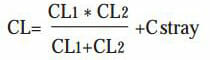
C stray includes the pin to pin input and output capacitance of the microprocessor chip at the Crystal 1 and Crystal 2 pins, plus any parasitic capacitances. As a rule of thumb, C stray may be assumed to equal 5.0 pF. Therefore, if CL1 = CL2 = 50pF, CL =30pF.
Trim Sensitivity: Trim sensitivity is a measure of the incremental fractional frequency change for an incremental change in the value of the load capacitance. Trim sensitivity (S) is expressed in terms of PPM/pF and is calculated by the following equation:
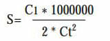
Where (Ct) is the sum of Co and CL.
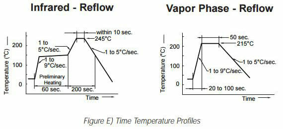
Solder Reflow of Surface Mount Devices: Mounting of SMD units is typically accomplished by means of solder reflow, as indicated in Figure E either by infrared heat or by vapor phase. The following graphs depicts the recommended times and temperatures for each of the two methods.
Soldering Characteristics: A variety of methods can be used to solder ECS products to P.C.B.s and substrates:
- Wave or Dual Wave
- Hot Air or Convection Flow
- Vapor Phase Reflow
- Infrared Reflow
- Bubble Solder Immersion
- Other (laser, etc.)
Due to the natural characteristics of material, some of our products cannot withstand heat shock. Extreme temperatures can cause tin (Sn) plating from the inside of the enclosure to reach its melting point, depositing solder on the quartz element. This can cause the component to oscillate at a lower frequency or fail completely. In other cases, solder contact can degrade, resulting in an open circuit. These problems can be avoided by preheating the components and board, and following the recommended soldering process time/temperature profiles noted above.
Note: It is important to check with your ECS factory representative before subjecting any crystal components to extreme environmental conditions.
Useful Crystal Equations:
Field Vibration: There are two basic types of vibration, periodic and random. Typically, vibration in the field produces complex waves of motion which can affect the output of quartz crystals. Most failures due to vibration occur as a direct result of mechanically amplified resonances, as higher acceleration levels are reached by resonant areas, resulting in higher potential for damage. All factors influencing vibrations should be thoroughly evaluated by using a prototype. Structural system, component location, mounting and encapsulation should all be considered to maximize stability. Remember that crystals are designed to withstand normal handling vibration; added ruggedizing may adversely affect desirable qualities such as stability tolerance or aging.