
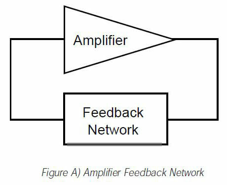
Crystal controlled oscillators may be considered as consisting of an amplifier and a feedback network that selects a part of the amplifier output and returns it to the amplifier input. You can view an example of such a circuit below.
A) The loop power gain must be equivalent to unison.
B) The loop phase shift must be equivalent to 0, 2Pi, 4Pi, etc. radians
The power fed back to the input of the amplifier must be adequate to supply the oscillator yield, the amplifier input and to overcome circuit losses.
The exact frequency at which an oscillator will operate is dependent on the loop phase angle shifts within the oscillator circuit. Any net modification in the phase angle will result in a change in the output frequency. As the usual objective of an oscillator to deliver a frequency that is essentially independent of variables, some means of reducing the net phase modification must be engaged. Conceivably the best and certainly the maximum common means of minimizing the net phase shift is to use a quartz crystal unit in the feedback loop.
The impedance of quartz crystal changes so dramatically, with changes in the applied frequency that all other circuit components can be considered as being of essentially continuous reactance. Consequently, when a crystal unit is used in the feedback loop of an oscillator, the frequency of the crystal unit will regulate itself so that the crystal unit presents a reactance which satisfies the loop phase necessities. A representation of the reactance vs. frequency of a quartz crystal unit is displayed below.
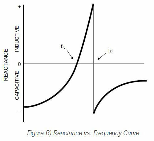
As is apparent from Figure B, quartz crystal unit has two frequencies of zero phases. The initial, or lesser of the two, is the series resonant frequency, commonly abbreviated as Fs. The subsequent or higher of the two frequencies of zero phases is the corresponding, or anti-resonant frequency, commonly abbreviated as Fa. Both the series and corresponding resonant frequencies appear resistive in an oscillator circuit. At the series resonant point, the resistance is minimal and the current flow is maximal.
At the parallel point, the resistance is maximal and the current flow is marginal. Consequently, the parallel resonant frequency, Fa should never be used as the governing frequency of an oscillator circuit.
A quartz crystal unit can be made to oscillate at any point along the line between the series and parallel resonant points by the inclusion of reactive components (usually capacitors) in the feedback loop of the oscillator circuit. Therefore, the frequency resulting from the addition of capacitance is higher than the series resonant frequency; it is usually called the parallel frequency, however it is lesser than the factual parallel frequency.
Just as there are two frequencies of zero phases associated with a quartz crystal unit, there are two principal oscillator circuits. These circuits are usually defined by the type of crystal unit to be used, namely “series” or “parallel”.
Series Circuit: A series resonant oscillator circuit uses a crystal which is designed to operate at its natural series resonant frequency. In such a circuit, there will be no capacitors in the feedback loop. Series resonant oscillator circuits are used primarily because of their minimal component count. These circuits may, nonetheless, provide feedback paths other than through the crystal unit. Thus, in the occurrence of crystal failure, such a circuit may remain to oscillate at some subjective frequency. A representation of a basic series resonant oscillator circuit is given below.
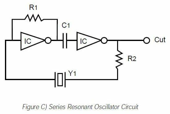
As is apparent from Figure C, a series resonant oscillator circuit provides no means of adjusting the output frequency, should modification be required. In the above circuit, resistor, R1 is exploited to bias the inverter and to produce it to operate in its linear region. This resistor also delivers negative feedback to the inverter. Capacitor C1 is a connector capacitor, used to block DC voltage. Resistor R2 is used to bias the crystal unit; therefore care must be taken that too small a value is not chosen. Crystal unit Y1 is a series resonant crystal unit, specified to function at the preferred frequency and with the desired frequency tolerance and stability.
Parallel Circuit: A parallel resonant oscillator circuit uses a crystal unit which is designed to operate with a specified value of load capacitance. This will create an outcome in which a crystal frequency with is higher than the series resonant frequency but lower than the true parallel resonant frequency. These circuits do not offer routes other than through the crystal unit to complete the feedback loop. In the occurrence of the crystal unit failure, the circuit will no longer continue to oscillate. A simple description of a parallel resonant circuit is given below.
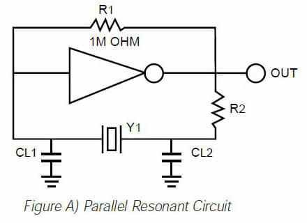
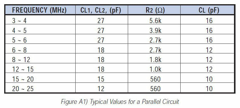
This circuit uses a solitary inverter, with two capacitors in the feedback loop. These capacitors encompass the “load capacitance” and together with the crystal unit, create the frequency at which point the oscillator will function. As the value of the load capacitance is altered, so is the output frequency of the oscillator. Thus, this circuit does provide a suitable means of adjusting the output frequency, should adjustment be required.
The resistors R1 and R2 serve the same functions as detailed for the series resonant circuit shown in Figure C. The two load capacitors, CL1 and CL2 assist to establish the frequency at which the crystal unit and therefore the oscillator will function. Crystal unit Y1 is a parallel resonant crystal unit, stipulated to operate with a specified value of load capacitance, at the preferred frequency and with the desired frequency tolerance and stability.
Reference has been made to a “specified load capacitance”. Load capacitance may be described as “the value of capacitance, measured or calculated, existing in the oscillator circuit, through the linking points of the crystal”. In the case of a series resonant circuit, there is no capacitance existing amongst the connecting points of the crystal unit and thus, load capacitance need not be stated for a series resonant crystal unit. In the instance of a parallel resonant oscillator circuit, capacitance is existent. As a direct dimension of this capacitance is unreasonable, it is frequently required to compute the value. The computation of the value of the load capacitance is done with the following equation:
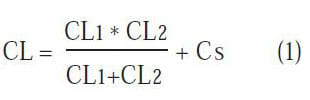
Where CL1 and CL2 are the load capacitors and Cs is the circuit vagrant capacitance, usually 3.0 to 5.0 pF.
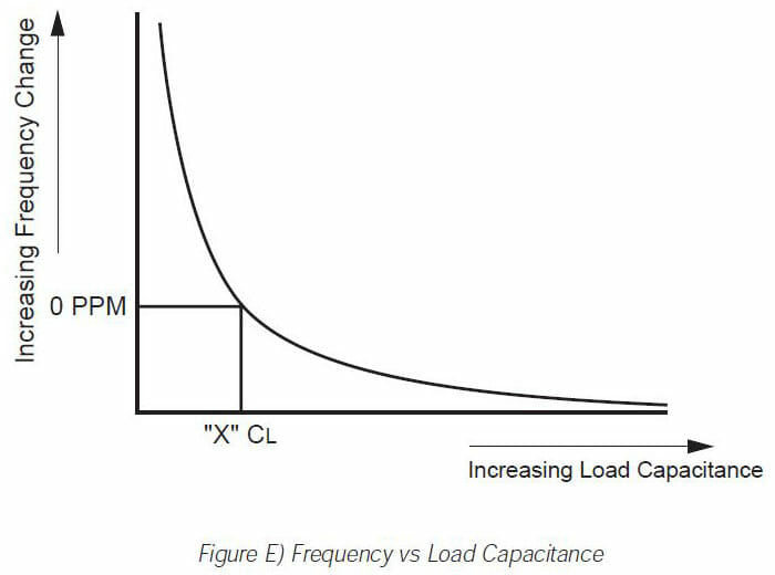
It must be noted that changes in the value of the load capacitance will result in changes in the output frequency of the oscillator. Thus, exact frequency control is required, and then a precise specification of load capacitance is required. To demonstrate, presume that a crystal unit is specified to operate at a frequency of 20.000 MHz with a capacity of 20.0 pF. Assume that the crystal unit is then placed in a circuit which presents an assessment of 30.0 pF. The frequency of the crystal unit will then be lower than the specified value. Contrariwise, should the circuit in question present an assessment of 10.0 pF; the frequency will be higher than the specified value. The association between and load capacitance is shown below.
Drive Level: The “drive level” is the power dissipated by the crystal unit while operational. The power is a function of the applied current and is usually expressed in terms of Milliwatts or Microwatts. Crystal units are specified as having certain maximum values of drive level, which transform as functions of the frequency and mode of operation. It is well to confer with the crystal unit vendor as to the maximum value of drive level allowed for a particular crystal unit. Exceeding the highest drive level for a given crystal unit may result in unstable operation amplified aging rates, and in some cases, catastrophic destruction. The drive level may be computed by the following equation:
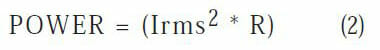
Where “I” is the rms current through the crystal unit and R is the maximum resistance value of the specific crystal unit in question. Equation (2) is simply “Ohms law” for power.
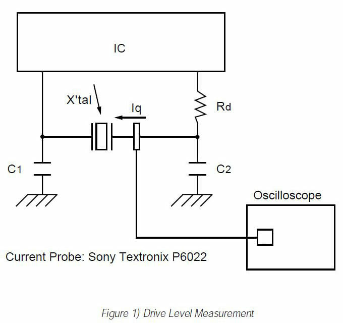
Measurement of the actual drive level in an operation oscillator circuit may be accomplished by temporarily inserting a resistor in series with the crystal unit. The resistor must be of the same ohmic value as the crystal unit. The voltage drop across the resistor may then be read and the current and power dissipation calculated. The resistor must then be removed. As an alternative means of measuring the drive level, a current probe may be used at the output lead of the crystal unit, space permits. The method is described below in Figure 1.
Frequency vs Mode: The frequency of a quartz crystal unit is limited by the physical dimensions of the vibrating quartz element. In some cases, the limiting dimensions (s) are the length and width. In the case of the most popular crystal unit, the “AT” cut crystal unit, the limiting dimension is the thickness of the vibrating quartz element. As the thickness is diminished, the frequency is increased. At some point usually around 30.000MHz, the thickness of the quartz plate becomes too thin for processing.
Should it be desired to develop an oscillator at a frequency higher than the limiting frequency, advantage must be taken of the fact that quartz crystal units will oscillate at odd integer multiples of their “fundamental” frequency. We may define the “fundamental” frequency as ‘that frequency which naturally occurs at a given set of mechanical dimensions”. Therefore, if a crystal unit has a fundamental frequency of 10.0 MHz it can also be made to oscillate at 3, 5, 7, etc. times the fundamental. That is, the unit will oscillate at 30.0. 50.0, 70.0, etc. MHz.
These multiples of the fundamental frequency are called “overtones” and are identified by the integer of multiplication, as in the “third overtone”, the “fifth overtone”, etc. When use at an overtone frequency is required, the crystal unit must be specified to operate at the desired frequency and on the desired overtone. One should never attempt to order a fundamental mode crystal until and then operate it at an overtone frequency. This is due to the fact that the crystal manufacturing processes differ for fundamental and overtone crystal units.
In many cases, the characteristics of the integrated circuit used in a particular oscillator design dictate that the fundamental frequency of the crustal unit be suppressed in order to ensure operation at the desired frequency and on the desired overtone. In such cases, it is usually necessary to modify the oscillator circuit. One method of modification is to add a “tank” circuit, consisting of an inductor and a capacitor. These modifications are shown in Figure F and G.
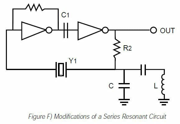
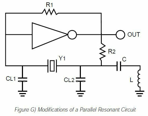
In both cases, the tank circuit is turned to resonate at some frequency between the fundamental and the desired frequency. This results in the unwanted frequency being shunted to ground, leaving only the desired frequency being present at the output of the oscillator.
Design Considerations: For good operation of an oscillator circuit, certain design considerations should be followed. In all cases, it is recommended that parallel traces be avoided in order to reduce circuit stray capacitance. All traces should be kept as short as possible and components should be isolated in order to prevent coupling. Ground planes should be used to isolate signals.
Negative Resistance: For optimum performance, an oscillator circuit must be designed in such a way to enhance “negative resistance,” which sometimes is called the “oscillation allowance”. Evaluation of the amount of negative resistance in a given circuit is accomplished by temporarily installing a variable resistor in series with the crystal unit. The resistor should be set initially at its lowest setting, preferably close to zero ohms. The oscillator is them started and the output monitored on an oscilloscope. The variable resistor is then adjusted so that resistance is increased while the output is continuously monitored. At some value of resistance, oscillation will be stopped. At this point, the variable resistor is measured to determine the ohmic value at which oscillation ceased. To this value, the maximum resistance of the crystal unit, as specified by the vendor, must be added. The total ohmic resistance is deemed to be the “negative resistance” or the “oscillation allowance”. For good, reliable circuit operation, it is recommended that the negative resistance be a minimum of five times the specified maximum resistance value of the crystal unit.
Values of negative resistance exceeding five times the maximum resistance of the crystal unit are better yet. As negative resistance tends to decrease at elevated temperature, it is recommended that the test be performed at the highest temperature of the operating range. See the special procedure illustrated below.
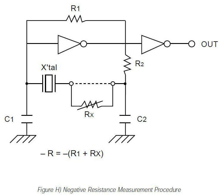
Procedures for Negative Resistance Measurement
1) Open either end of the crystal unit in the main circuit used, and insert a variable resistor in series with the crystal unit, as shown. Change the resistance value to examine the limits of oscillation and resistance in ohms observed at that time. In this case power must be turned on and off, without fail.
2) Negative resistance (-R) in the circuit is the sum of the value obtained by Step 1) above and the resonant resistance R1 of the crystal.
Note: This measurement should be carried out at both the upper and lower limits of the operating temperature range.
3) C1 and C2 should be used within the range of 10 ~ 30 pF. If C1 and C2 are used below 10 pF or above 30 pF, oscillation performance may be easily affected. Drive Level may increase, or negative resistance may decrease, thus failure to maintain oscillation.