
Written by David Meaney, Vice President of Global Technical Sales and Marketing and Dean Clark, European Director of Operations at ECS Inc. International
When laying out your printed circuit board to accept components and give them the best possibility to perform at their best is a complicated task, such as clocking signals and their routing. If we follow some industry standard rules, electromagnetic interference problems can be minimized without the need for complicated formulas and expensive simulation tools.
The reason PCB layout becomes more and more important is because of the trend to reduce board size and increase integration. Smaller form factors, and lower power electronics, all lead to further considerations. The higher the switching frequencies the more radiation will be generated. With good layout, many EMI problems can be minimized to meet the required specifications. Listed below are some recommendations that ECS Inc. International suggest you follow as good engineering practice.
Crystal Printed Circuit Board (PCB) Design Guidelines
- Connect the crystal and external load capacitors on the PCB as close as possible to the oscillator input and output pins of the chip.
- The length of traces in the oscillation circuit should be as short as possible and must not cross other signal lines.
- Avoid right angle bends on traces
- Ensure that the load capacitors CX1, CX2, and CX3, in case of third overtone crystal usage, have a common ground plane.
- Loops must be made as small as possible to minimize the noise coupled in through the PCB, and to reduce any parasitics as much as possible.
- Do not lay out the ground (GND) pattern under crystal unit.
- Do not run Digital / RF signal lines or power under crystal unit for multi-layered PCB.
Oscillator Printed Circuit Board (PCB) Design Guidelines
- Layout the oscillator footprint on the PCB as close as possible to the input pins of the load or chip.
- The length of traces should be as short as possible and must not cross other signal lines.
- Avoid right angle bends on traces. Capacitance increases in the 45° corner region changing the characteristic impedance of the trace, leading to reflections. This can be mitigated by rounding right angles.
- Use series termination to reduce standing waves between source and termination. This is constructed by inserting a resistor in series as close to the output pin of the oscillator as possible. For proper impedance matching the output impedance of the clock driver plus series termination resistor should be equal to the trace impedance.
- Keep differential output traces as close to the same length and as close as possible. This increases the coupling factor between the traces, bringing noise into the common mode, which is less problematic for a differential input stage.
- A good practice is to have the oscillator connected to the common ground plane.
- Do not lay out the ground (GND) pattern under crystal unit, this adds parasitic capacitance.
- Do not run Digital / RF signal lines or power under oscillators for multi-layered PCB, as this will add noise.
Pierce Oscillator Layout
The points above are important for the application of pierce oscillators as used by microprocessors. See below the circuit and a typical layout for a pierce oscillator using a 4-pad crystal.
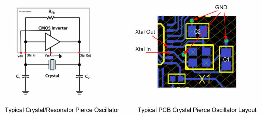
The crystal oscillator loop has a low input impedance at the oscillator frequency, but a high input impedance characteristic outside of the resonance frequency range.
This high impedance characteristic is vulnerable to EMI when an electrical field is applied in its vicinity. Newer technology has seen the oscillator signal level restricted at <1V, making it more susceptible.
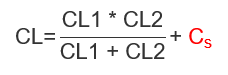
To highlight the importance of keeping the stray PCB capacitance low, highlighted is the Cs in the calculation. The lower the CL of the crystal, the more impact the stray PCB capacitance has on the design.
The ground connections to the load capacitors C1 / C2 should be kept as short as possible to avoid ground currents with other circuits. Very often the XTAL IN and XTAL OUT pins are adjacent on the processor. Parasitic capacitance can be an issue, so traces should be routed as far apart as possible whilst keeping them as short.
Typical capacitances seen might be:
– XTAL IN to ground: 1pF
– XTAL OUT to ground: 2pF
– XTAL IN to XTAL OUT: 0.5pF
Most common crystal types have seam sealed cases, in which the case lid is connected electrically to the ground pins. With this type of package there is a recommendation to ground the pins to reduce the potential of EMI from the lid. It should be noted that seam sealed packages offer better performance. The alternative sealing method is a glass sealed crystals, and due to this process, the lid is isolated from the ground pins. With this type of package, it’s not recommended to ground the ground pins on the crystal.
Electromagnetic Compatibility (EMC)
Electromagnetic Compatibility is the ability of electrical components, equipment, and systems to function as designed in their environment. This is done by limiting the unintentional generation, propagation, and reception of electromagnetic energy. These unwanted sources of noise are known as electromagnetic interference (EMI). The goal of EMC is the correct operation of different equipment in a common electromagnetic environment.
The Ground Plane
A ground plane is effective when in use with an analog or digital circuit and a mixture of components. Ground connections are made as needed rather than uniformly across the layout.
A ground plane is not created by simply filling all empty space with copper and connecting it to the ground. Its function is to allow the flow of return current, and the ideal layout should have minimum interruptions to it. Therefore, multilayer boards are used. An entire uniform layer can be devoted to Ground, one to power, and another to signaling. This enhances the distribution of interlayer capacitance. It also has the additional benefit of low impedance between power and ground at high frequencies.
Individual holes make no difference to the ground plane, but large slots do. When the ground plane is interrupted by other tracks or holes the normal low-inductance current flow is diverted around the obstacle and the inductance is effectively increased.
Interruptions should only be tolerated if they do not cut across lines of high di/dt flow. Tracks underneath components carrying high switching currents or fast logic edges will cause induced capacitance. Even a very narrow track interconnecting two segments of ground plane is better than none. At high frequencies, and this includes digital logic edge transitions, current tends to follow the path that encloses the least magnetic flux. This means that the ground plane return current will prefer to concentrate under its corresponding signal track.
Some board manufacturers do not recommend leaving large areas of copper because it may lead to board warping or crazing of the solder resist. If this is likely to be a problem, you can replace solid ground plane by a cross-hatched pattern without degrading its effectiveness. To make a soldered connection to the ground plane, or any other large area of copper on the surface of the board, you should “break out” the solder pad from the ground area and connect using short lengths of track. This prevents the ground plane from acting as a heat sink during soldering for reliable joints.
Electromagnetic Interference (EMI)
Radiated — EMI
What is Radiated Emissions (or EMI) Testing?
Radiated emissions testing involves measuring the electromagnetic field strength of the emissions that are unintentionally generated by your product. Emissions are inherent to the switching voltages and currents within any digital circuit. This will let you know what the level of emissions are, and then you can determine if they will affect the performance of your system or surrounding systems.
Typical Radiated Failure Modes
There are virtually an unlimited number of designs or electromechanical ways that you can cause radiated emissions. Here is a short list of some typical EMI design issues:
- Noise on the cabling
- Poor board grounding
- Non-optimized layer stack
- Ineffective board decoupling
- Poor cable termination
- Poor signal integrity
- Noisy power supply
- Component placement
- Cuts in return paths
- Large current loops
- Grounding for heat-sinks & LCDs
- Segmented ground fills
- Signals close to edge of reference plane
- Decoupling capacitor placement
- Poor board grounding
- Decoupling capacitor
- Ineffective board decoupling
- Segmented ground fills
- Poor signal integrity
- Large current loops
- Component placement
Conducted — EMI
Every electronic device creates electromagnetic energy and a certain portion of it will be conducted onto the power supply and potentially coupled to the external power supply.
In order to restrict the amount of interference your device can couple back onto a power supply; test labs measure these emissions. Typically, they are interested in emissions in the bandwidth of
150 kHz ~ 30 MHz. They check for radiation and verify that they comply with specified limits.
EMI testing procedures and levels are governed by the CISPR: International Special Committee on Radio Interference. For more information please visit International Electrotechnical Commission at https://www.iec.ch/emc/iec_emc/iec_emc_players_cispr.htm
Emissions Testing
In accordance to ANSI C63.4, the LISN (or LISNs) sit on the ground, while your product sits on a table (or remains floor standing if the equipment is large).The RF port of a LISN connects directly to a spectrum analyzer (or via a transient limiter to prevent damage from voltage spikes).
Conducted Emissions Applicability
Conducted emissions testing is usually performed on devices that connect to an AC power supply. That is regardless of whether you’re using a pre-certified AC-DC power supply adapter. For some standards, there are also limits placed on devices that operate from a DC power supply.
Conducted Emissions Recommendations
Without going into huge detail on circuit design for conducted emissions compliance, there are a few simple ways that you can minimize the risk of failing conducted emissions testing:
- Always source a power supply that is rated for the limits that you need to pass
- If your device is a ‘class B’ device, then make sure to source a class B adapter. An adapter that has only passed class A limits, is unlikely to result in a system pass. A class B adapter doesn’t guarantee a class B conducted emissions pass, but it will certainly help.
- Similarly, for stricter military, medical, automotive or aerospace limits, always source a supply who’s specification claims compliance with the relevant limit.
- Bring at least 3 different power supplies to the test lab
- If your device uses an external AC-DC power adapter, bring equivalents from different manufacturers just in case. If you fail, you can swap it out and see if the other supplies result in a pass.
- Check your power supply rails for ripple.
- If you have nice clean power supplies, the chances are that your PDN and decoupling are in good shape. If you see excessive ripple or spikes from switching power supplies, this noise may well be present at the AC side of your power supply.
- If there is an essential reason to split the ground plane, such as to separate analog and digital grounds to avoid noise coupling, be cautious because splitting ground planes can act as slot antennas and radiate. In these cases, only connect split ground planes at a single point. The more common ground connections you have, the more loops you create, and the more EMI your design will radiate.
- Many designs will have bypass and decoupling capacitors; you can reduce the return current path by connecting them to ground. This reduces the size of the ground loop, and therefore the radiation. Just be sure not to connect a bypass capacitor between a power plane and an unrelated ground plane, which can cause capacitive coupling.
For more technical resources, please reference our library of technical guides, educational video library on frequency control and product information, our reference design library or our current product catalog.
Please contact us if you need additional information or have a specific requirement in your application.
ECS Inc. International
15351 West 109th Street
Lenexa, KS 66219
Tel: 913-782-7787
Toll Free: 1-800-237-1041
Fax: 913-782-6991