
Written by David Meaney, Vice President of Global Technical Sales and Marketing and Dean Clark, European Director of Operations at ECS Inc. International
What is an Oscillator?
An oscillator is an electronic circuit which generates a repetitive signal. This signal can be in many forms depending on the application. Some applications require a basic clock to maintain operational intervals for processes. Other applications require a clock with very clean waveform and tight stability to produce high quality communications and data transfers.
In analog applications such as RF radio transceivers that use a superheterodyne to receive and transmit signal chains, will typically find sinusoidal output waveforms. A sine wave is a continuous wave that represents a smooth periodic oscillation. In RF communication, the oscillators sine wave output provides an accurate, low noise frequency reference to the transceiver.
In digital electronics we see square wave outputs. Square waves are a waveform that alternate from minimum to maximum amplitude at a steady frequency. An ideal square wave would have the minimum and maximum periods at equal duration, and this would have a 50/50% duty cycle. In practice, there will be some variation in duty cycle, so 45/55% or 60/40% may be more typical. A square wave output signal has many uses but is extensively used to time the execution of instructions in a circuit or microprocessor.
Oscillators
Oscillators can have several different types of resonators associated with them. The most prolific and best performing of these is quartz. You may also find oscillators that use ceramic, SAW[1] or MEMS[2] based resonators to be the starting point for the operational frequency. They use mechanical vibration or tuned cavities to generate the clock signal. In the case of the quartz-based oscillator, the composition of the quartz material, and the angles that the crystal are cut makes this type of oscillator very precise and stable over a wide temperature range. The process for making oscillator grade crystal blanks is time consuming, with many steps to ensure consistent high-quality product, but they offer vastly superior stability over RC oscillators.
Oscillator Principles
The principle behind the oscillator circuit is a stable steady state output signal. One way to accomplish this is by using a positive feedback loop. Here a portion of the output voltage is feedback to the input with no net phase shift, so reinforcing the output signal. The signal is then amplified and looped back again causing the output signal to grow. The gain in the feedback loop needs to be controlled to unity gain, otherwise the signal will be clipped and distorted.
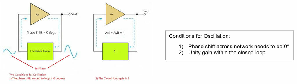
Figure 1 – Oscillator Feedback Loop Showing Conditions for Oscillation
In Figure 1, we see a simplified feedback oscillator loop showing that a basic oscillator circuit consists of an amplification stage and a feedback network that acts as a filter that decides what the feedback loop gain should be.
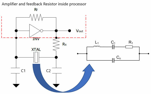
Figure 2 – Pierce Oscillator design using Processor with inverter and feedback resistor.
Figure 2 shows a Pierce Oscillator design commonly used in digital processor designs. In this type of crystal oscillator design, the filter consists of the crystal’s equivalent model and the external load capacitors. The exact frequency at which an oscillator will operate is dependent on the loop phase angle shifts within the oscillator circuit. Changes in the phase angle will result in a change in the output frequency.
Start-up Time
Startup time is the period when an oscillator is first turned on. During this period there will be instabilities until the oscillations stabilize. Start-up time is usually measured in microseconds (µS), but it is frequency dependent and controlled by the feedback loop. The magnitude of the closed loop gain has great influence on the startup time. Factors that negatively affect closed loop gain include the low drive level, higher values of crystal capacitive load (CL), and equivalent series resistance (ESR). Low gain can cause excessively long start-up time, and too high of gain can cause start-up to fail altogether or over drive the crystal structure. The ideal gain is dependent on the negative resistance of the oscillator circuit, where the drive must overcome the negative resistance to start-up and build the oscillator output. Because of this the oscillator frequency directly influences the start-up time, so the time it takes to circulate the loop is considerably longer for a KHz oscillator than a MHz oscillator. Poor gain margin is a common problem in kHz oscillators, since drive levels are an order of magnitude lower and crystal ESR’s an order of magnitude higher. To overcome these issues careful design is required to match drive levels to suitable CL and ESR values.
Reactance
The impedance of quartz crystal changes so dramatically with changes in the applied frequency, that all other circuit components can be considered as being of essentially continuous reactance. Consequently, when a crystal unit is used in the feedback loop of an oscillator, the frequency of the crystal unit will regulate itself so that it presents a reactance which satisfies the loop phase gain. A representation of the reactance vs. frequency of a quartz crystal unit is displayed in Figure 3.
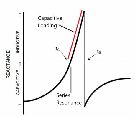
Figure 3 – Reactance vs. Frequency Curve
A quartz crystal unit can be made to oscillate at any point along the line between the series and parallel resonant points by the inclusion of reactive components (see Figure 3, line marked Capacitive Loading), such as capacitors in the feedback loop of the oscillator circuit. The frequency resulting from the addition of capacitance is higher than the series resonant frequency; it is usually called the parallel frequency however it is lesser than the factual parallel frequency. Since there are two frequencies of zero phases associated with a quartz crystal unit, there are two types oscillator circuits. These circuits are defined by the type of crystal to be used. They are either series resonant or parallel resonant.
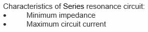
Series Circuit
In a balanced LC circuit, the resonant frequency is the frequency at which the reactance of the inductance and the reactance of the capacitance cancel each other out leaving just the resistive value. Figure 4 shows the series resonant circuit.
Figure 4 – Series Resonant Circuit
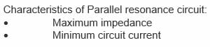
Parallel Circuit
A parallel resonant Oscillator circuit uses a Crystal unit which is designed to operate with a specific value of load capacitance. This will create an outcome in which a Crystal frequency with is higher than the series resonant frequency, but lower than the true parallel resonant frequency. These circuits do not offer routes other than through the Crystal unit to complete the feedback loop. In the occurrence of the Crystal unit failure, the circuit will no longer continue to oscillate. A simple description of a parallel resonant circuit is given below.
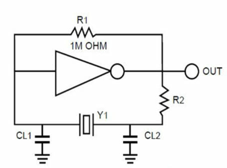
Figure 5 – Parallel Resonant Circuit
Adjusting Frequency “Pulling”
A crystal can be “pulled” from its series frequency by adding reactance (capacitance) in series with the crystal. When operated in combination with an external load capacitance (CL) the crystal oscillates in a frequency range slightly above its series resonant frequency. This is the parallel (load resonant) frequency. When ordering a parallel crystal, always specify the nominal parallel resonant frequency and specify the circuit load capacitance in Pico Farads (pF).
Approximate equation for crystal pulling limits is:
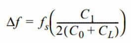
The limits of ∆f depend on the crystal Q and stray capacitance of the circuit. If the shunt capacitance, motional capacitance, and load capacitance is known, the average pulling per pF can be found using:
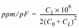
The capacitance can be changed by using a varactor diode, where the pulling can be done electrically to change the value of capacitance. This is used in VCO’s, VCXO’s and VCTCXO’s to pull the frequency.
Load Capacitance
Load capacitance is the amount of external circuit capacitance in parallel with the crystal itself. In this example we see that the crystals parallel resonance mode is always above the series resonance frequency and is characterized by inductive reactance. In parallel resonance oscillation mode, the crystal’s inductance (motional inductance) is in parallel with the oscillator’s load capacitance, thereby forming an LC tank circuit. This LC determines the oscillator frequency.
When specifying a series resonant crystal, load capacitance can be ignored since the crystal’s motional inductance and motional capacitance are the only LC components that determines oscillation frequency.
CL can be determined by the formula:

For example, where CL1 and CL2 are the load capacitors and CS is the circuit stray capacitance, usually 3pF ~ 5pF. It must be noted that changes in the value of the load capacitance will result in changes in the output frequency of the oscillator.
If exact frequency control is needed, then a precise specification of load capacitance is required. To demonstrate, presume that a crystal unit is specified to operate at a frequency of 20MHz with a capacity of 20pF. Assume that the crystal unit is then placed in a circuit which presents an assessment of 30pF.
The frequency of the crystal unit will then be lower than the specified value. Contrarily, should the circuit in question present an assessment of 10pF, the frequency will be higher than the specified value. The association between frequency and load capacitance is shown in Figure 6.
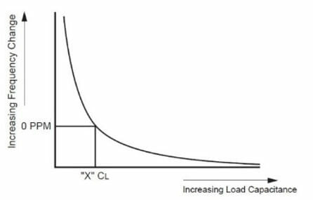
Figure 6 – Frequency vs. Load Capacitance
Drive Level
The drive level is the power dissipated by the crystal unit while operational. The power is a function of the applied current and is usually expressed in terms of milliwatts (mW) or microwatts (µW). Crystal units are specified as having certain maximum values of drive level, which transform as functions of the frequency and mode of operation. Exceeding the highest drive level for a given crystal unit may result in unstable operation, including accelerated aging rates, and in some cases, complete crystal failure. The drive level may be computed by the following equation:
POWER = (Irms2 * R)
Negative Resistance
For optimum performance, an oscillator circuit must be designed in such a way to enhance negative resistance, which sometimes is called the oscillation allowance. Determining the amount of negative resistance is accomplished by putting a variable resistor in series.
Evaluation of the amount of negative resistance in each circuit is accomplished by temporarily installing a variable resistor in series with the crystal unit. The resistor should be set initially at its lowest setting, preferably close to zero ohms. The oscillator is then started, and the output monitored on an oscilloscope. The variable resistor is then adjusted so that resistance is increased while the output is continuously monitored. At some value of resistance, oscillation will be stopped. At this point, the variable resistor is measured to determine the ohmic value at which oscillation is ceased. To this value, the maximum resistance of the crystal unit, as specified by the vendor, must be added. The total ohmic resistance is deemed to be the negative resistance or the oscillation allowance.
For good, reliable circuit operation, it is recommended that the negative resistance be a minimum of five times the specified maximum equivalent series resistance value of the crystal unit. Values of negative resistance exceeding five times the maximum resistance of the crystal unit is even better. As negative resistance tends to decrease at elevated temperature, it is recommended that the test be performed at the highest temperature of the operating range.
Oscillator Transconductance
Another way to consider if the oscillator will start up consistently is to consider the transconductance. To ensure oscillation starts and reaches a stable phase, the oscillator must provide enough gain to compensate for the oscillation loop losses and to provide the energy for the oscillation build up. As discussed in the “Start-up Section”, the ratio between oscillator gain and oscillation loop critical gain cannot just exceed 1, as this would induce a too long oscillator startup time or even stop start-up altogether. Designers should try to meet a gain margin of greater than 5. These parameters are determined by the formula gain margin = gm / gmcrit ≥ 5 gm is the oscillator transconductance specified in the IC datasheet.
For MHz oscillators the transconductance is in the range of a dozen of mA/V, while for kHz oscillator transconductance ranges from a few to a few dozens of µA/V, depending on the product.
gmcrit is defined as the minimal transconductance of an oscillator required to maintain a stable oscillation.
Assuming the design is using equal CL1 and CL2 values, and that the crystal load is the same as the crystal CL, gmcrit is expressed as follows:
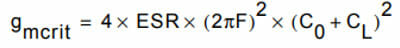
When considering start-up of the oscillator, choice of crystal parameters is important; lowering the ESR, frequency, C0, and CL will reduce gmcrit, and so maximize the gain margin.
Frequency vs. Overtone Mode
The frequency of a quartz crystal unit is limited by the physical dimensions of the vibrating quartz element. In some cases, the limiting dimensions are the length and width. The most popular crystal unit is the AT cut crystal. The limiting dimension is the thickness of the vibrating quartz element. As the thickness is reduced, the frequency goes up. At some point, usually around 50MHz, the thickness of the quartz plate becomes too fragile for use in the field.
If you need to develop an oscillator at higher frequencies that will still be robust enough to operate in the field, we can look at using one of the other resonant frequencies. These are lower magnitude frequencies that are generated as harmonics. These harmonics will all be at odd integers of the fundamental frequency. Therefore, if a crystal unit has a fundamental frequency of 10MHz, it can also be made to oscillate at 3x, 5x, 7x, etc. times the fundamental. That is, the unit will oscillate at 30MHz, 50MHz, and 70MHz, etc. These multiples of the fundamental frequency are called overtones and are identified by the integer of multiplication, as in the third overtone, the fifth overtone, the seventh overtone, etc. When use at an overtone frequency is required, the crystal unit must be specified to operate at the desired frequency and on the desired overtone. One should never attempt to order a fundamental mode crystal unit and then operate it at an overtone frequency. This is because the crystal manufacturing process is different for fundamental and overtone crystals.
In many cases, the characteristics of the integrated circuit used in an oscillator design dictate that the fundamental frequency of the crystal be suppressed in order to ensure operation at the desired frequency and not at the more powerful fundamental frequency. It is necessary to modify the oscillator circuit. One method of modification is to add a tank circuit, consisting of an inductor and a capacitor. These modifications are shown in Figure 7 and Figure 8, for series and parallel resonant circuits.
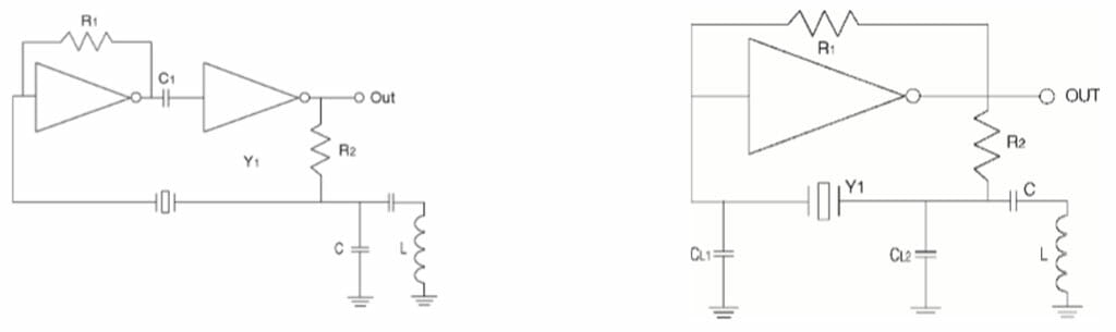
Figure 7 – The modification of a Series resonant circuit
Figure 8 – The modification of a Parallel resonant circuit
In both cases, the tank circuit is tuned to resonate at some frequency between the fundamental and the desired frequency. This isolates the desired frequency and shunts the rest to ground, leaving only the desired frequency at the output of the oscillator.
Design Considerations
When designing an oscillator circuit or laying out your board for and oscillator, certain design considerations should be followed. It is always recommended to avoid parallel traces in order to reduce tray capacitance. All traces should be kept as short as possible and components should be isolated in order to prevent coupling. Ground planes should be used to isolate signals.
There are many other terms that you will need to familiarize yourself with during your design efforts. ECS. Inc has a broad line of frequency control and magnetics products to choose from. There is also an extensive library with technical guides, video learning, and reference designs that you can review.
[1] SAW, – Surface-Acoustic-Wave (SAW) resonator. A 1-port SAW resonator has one IDT (Inter Digital Transducer) that is fabricated on a quartz substrate, it generates and receives SAW. The design has two grating reflectors, these reflect SAW and generate a standing wave between the two reflectors. It is then converted back to an electrical signal.
[2] MEMS – Micro-Electromechanical System. A MEMS resonator is a silicon device that uses nanometer resonant structure to create a vibrating structure.
For more technical resources, please reference our library of technical guides, educational video library on frequency control and product information, our reference design library or our current product catalog.
Please contact us if you need additional information or have a specific requirement in your application.
ECS Inc. International
15351 West 109th Street
Lenexa, KS 66219
Tel: 913-782-7787
Toll Free: 1-800-237-1041
Fax: 913-782-6991