
Written by David Meaney, Vice President of Global Technical Sales and Marketing at ECS Inc. International
What Are Phase Noise and Jitter, and How Are They Connected?
The advancing ability to communicate and move data on a global scale makes our planet seem smaller every day. With an ever-increasing demand for faster cellular and internet speeds, we are seeing data transmission rates growing at an exponential rate. As these data rates increase, they must push the current limitations of timing margins. Timing margin is the clean, usable bandwidth that providers use for all their subscriber-paid traffic. As you can imagine, cleaner bandwidth is equal to more data; more data equals more customers on the same network—which, in turn, equates to more profit.
When trying to use the fringe of the timing margin, two different but connected anomalies occur. These anomalies will be phase noise and jitter. They are both significant detractors to clean clocking. The significance of them will depend on your method of data transmission. RF engineers will generally look at phase noise while digital designers are more likely to focus on jitter.
Phase noise and jitter are, as previously stated, detractors from clean clocking. Therefore, both are indicators of frequency quality and the integrity of a timing signal. At the root of their function, they are related to each other. If we look at these two anomalies, we can characterize the timing instability in a clock or data stream at a system level.
Phase noise is defined as the electrical noise caused from the short-term phase fluctuations that occur in a signal. These random fluctuations are caused by time domain instabilities called jitter.
Jitter is defined as a deviation of the signal pulses in a high-frequency signal. The deviation can be in terms of amplitude, phase timing or the width of the signal pulse.
Phase noise and jitter are two different measurements of the same information about clock performance. Phase noise being the measured performance in the frequency domain and jitter being the measured performance in the time domain.
Let’s take a closer look at the definition and measurement of phase noise and jitter as they are applied to timing in electronic circuits.
What is Phase Noise
Phase noise is the measurement of noise spectrum on either side of a signal, adjacent to the center frequency or fundamental clock in the frequency domain. Phase noise is the result of jitter that is generated because of random phase variations of the signal. The levels in signal phase or frequency are portrayed in the bandwidth of the spectral line. The greater the timing instability, the broader the spectral line. To define phase noise, three elements need to be specified:
- Phase noise amplitude: The level or amplitude of phase noise specification is expressed in dB relative to the carrier. This is normally denoted as dBc, for example, -50dBc is 50 decibels down in level from the carrier. This method of measurement is adopted because the phase noise normally varies in line with the carrier level. Where the phase noise varies with the carrier level, the specification can state that the phase noise is – n dBc at a given carrier level.
- The offset from the carrier: An essential part of the phase noise specification is the offset from the carrier at which the phase noise was a certain level. This is because the noise level varies according to the frequency offset from the carrier, and the frequency offset must be given by the component supplier. Typically, the phase noise rises much faster as it gets closer to the carrier and falls away until it ultimately reaches a noise floor. Offsets of 1 kHz, 10 kHz, 100 kHz, etc. are commonly quoted offsets.
- The measurement bandwidth: The noise power is proportional to the bandwidth and therefore it is necessary to state the bandwidth that has been used. The wider the bandwidth that is used, the greater the level of noise that will pass through the filter and be measured. The most convenient bandwidth to use is 1 Hz because it is easy to relate this level to other bandwidths. As a result, this phase noise specification format has been almost universally adopted. Spectrum analyzers are unable to measure in a 1 Hz bandwidth directly because this would require a very narrow filter bandwidth. Therefore, they measure the signal in a wider bandwidth and mathematically adjust the level to that of a 1 Hz bandwidth.
A typical phase noise specification for a signal generator or other oscillator may be -100 dBc/Hz at a 100 kHz offset. For a complete phase noise specification, several points will be specified to give an indication of the phase noise at different points, typically at points varying by a factor of ten: 10 Hz, 100 Hz, 1 kHz, etc.
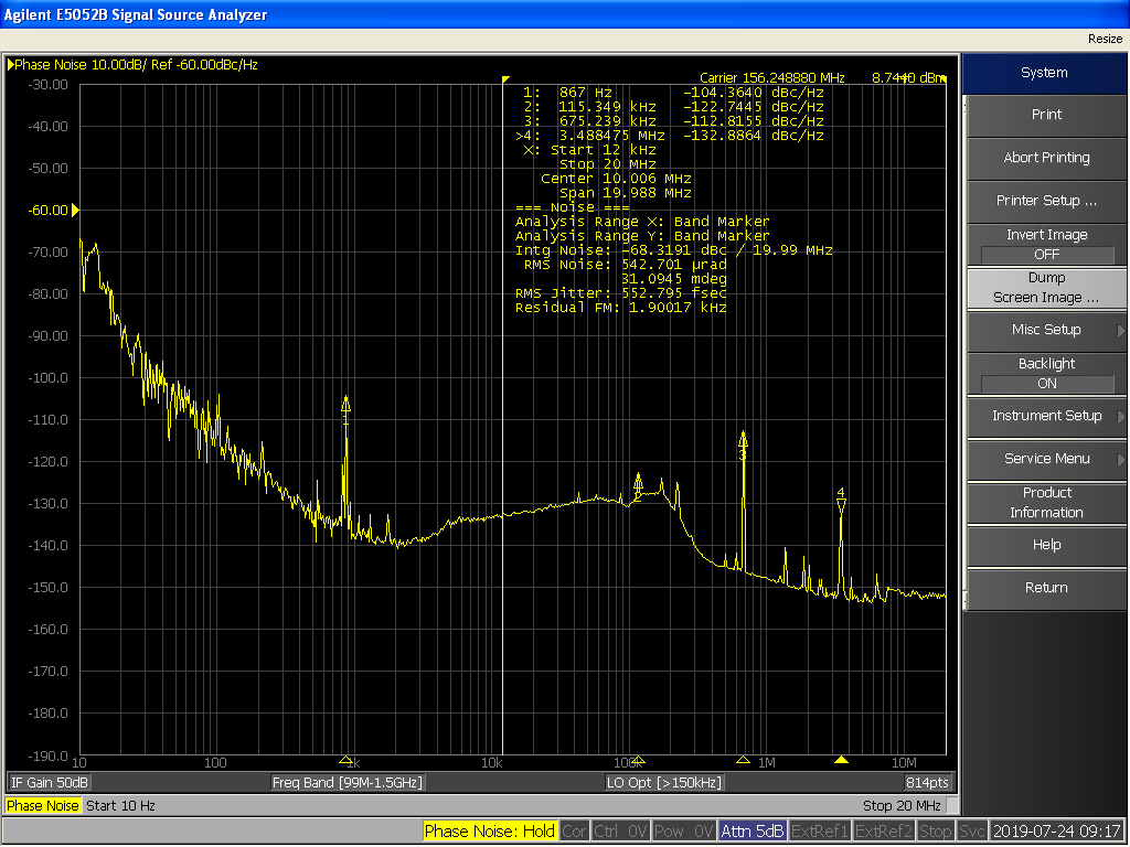
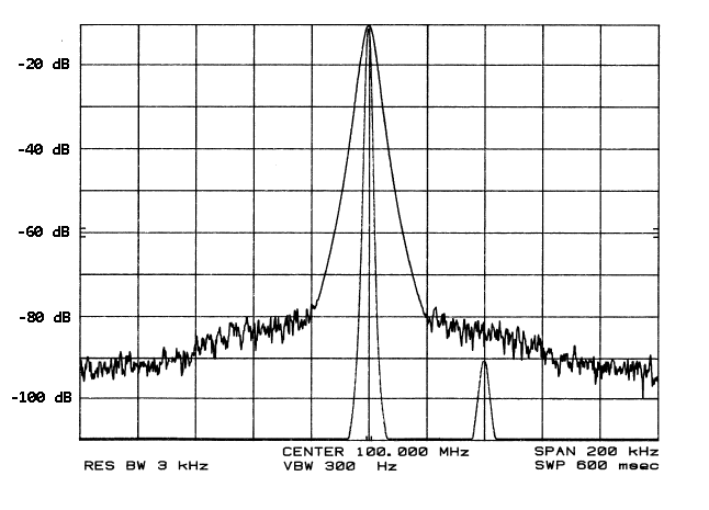
Figure 1. Phase noise plot as seen on a spectrum analyzer and oscilloscope graph.
Phase noise is present on all signals at some level. In most applications, the level of phase noise is not particularly important, but in others, like SONET, RF communications and cellular communications, it can be essential to the overall operation of the system. The amount of phase noise can be mitigated with proper oscillator selection and where they are used. With improvements needed to keep up with the requirements for radio systems of all types, phase noise is a parameter that is of increasing importance.
What is Jitter
Jitter is the inconsistency of a signal’s cycle-to-cycle period from its perfect symmetry. It can take several forms: Edge or phase jitter is measured as time interval error and period, or cycle-to-cycle, jitter is the difference between the periods of adjacent cycles. Jitter can be measured and defined in two variations: random jitter or deterministic jitter. Random jitter is generally unconnected because the peak jitter values increase with time. Deterministic jitter elements are connected and do not increase with time. The oscilloscope plot below shows the jitter.
How to Measure Jitter
One of the most critical aspects of clock performance is jitter. Unfortunately, there is no industry standard to measure jitter however, there are several accepted methods for determining the level of jitter in clocks. These results can vary significantly depending on the test equipment that is used, how they are connected and what the actual test conditions are. While the JEDEC standards do provide definitions and suggested test conditions, there is a lack of consistency between measurements from different testers.
There are three elements that are part of all the different types of jitter testing:
- Device under test (DUT) – This is the component you want to measure.
- Reference oscillator – System clock needs to have better stability performance the DUT.
- Power supply – Clean power offers accurate and repeatable testing.
Tests should be performed using calibrated measurement equipment such as:
- Oscilloscope
- Frequency counters
- Signal integrity analyzer
Making Time Domain Jitter Measurements
Time domain jitter measurements can be made with an oscilloscope. Oscilloscopes offer easy viewing of waveforms and pulses. Most vendors offer jitter measurement test packets at an additional cost. A high-speed (1GHz+) oscilloscope that has a high sampling bandwidth (10GS/s+) should be enough to gather the desired data. Keep in mind that time domain jitter measurements, specifically period and cycle-to-cycle, are random and given as a mean value over a number of samples. JEDEC standard 65 requires a minimum of 1,000 samples, but a 10,000-sample rate seems preferred by most engineers.
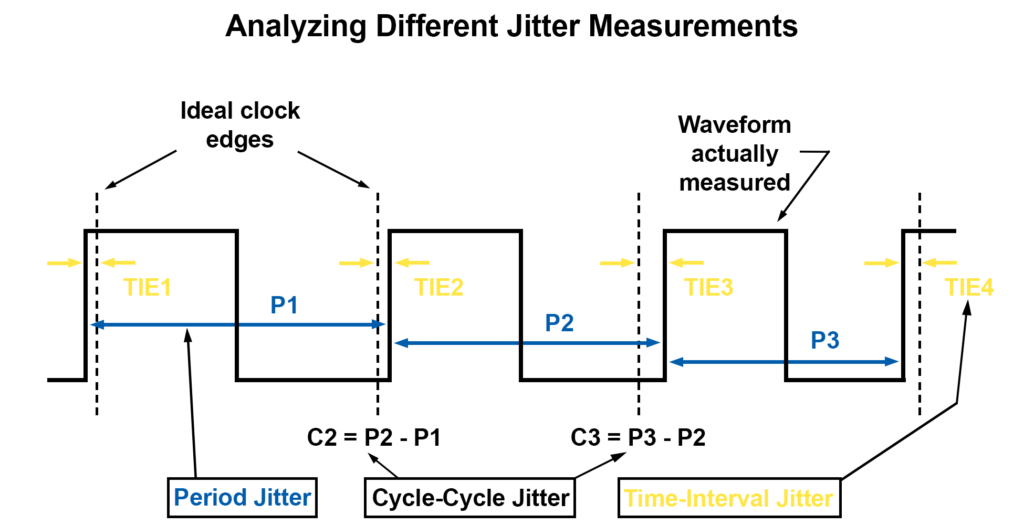
Period Jitter
Period jitter is the difference between a measured clock period and the ideal period. An ideal period may be difficult to discern so it is more practical to treat the average observed period as the ideal period. This is a common practice for timing device manufacturers to provide more accurate specifications. The standard procedure for measuring period jitter involves randomly measuring the duration of one clock period 10,000 times and using the recorded data to calculate the mean, standard deviation and peak-to-peak values. Due to the random nature of period jitter, the peak-to-peak values can vary greatly. Period jitter may need to be retested a few times to get a true average value.
Cycle-to-Cycle Jitter
The procedure for measuring cycle-to-cycle jitter requires measuring the duration of two full clock periods 10,000 times and taking the difference between the two. The recorded data is used to calculate the mean and standard deviation values. The peak value is simply the largest difference in periods observed. As previously stated, when determining period jitter, peak-to-peak values can vary greatly so often times cycle-to-cycle jitter needs to be retested several times to come up with an average value.
Time Interval Error (TIE) Jitter
Measuring TIE jitter is very difficult when only utilizing an oscillator. Typically, a histogram is necessary to plot the measurement values against the frequency of occurrence of the measurements. An example of a jitter histogram for a TIE measurement is shown below. In this case, the continuous variable is mapped into 500 bins and the total population of the data set is 3,200,000. The mean value of TIE is theoretically zero and as can be seen in this measurement, the mean value is 0 nsec. For this plot, the distribution is approximately Gaussian with a standard deviation of 1.3 psec.
Phase Noise, Jitter and Frequency Control Components
The presence of phase noise and jitter can significantly degrade the performance of various applications, such as wireless communication, high-speed data transmission and radar systems. They can introduce errors, reduce signal quality and limit the achievable data rates and transmission distances. To mitigate the adverse effects of phase noise and jitter, accurate frequency control components are essential. These components provide stable reference frequencies, precision frequency tuning and low phase noise characteristics to minimize timing errors and maintain signal integrity.
PLLs and frequency synthesizers are widely employed to attempt precise frequency control and reduce phase noise and jitter in complex systems. These techniques will use feedback loops and advanced filtering to synchronize the output frequency with a stable reference, minimizing phase noise and associated jitter. However, the selection and design of frequency control products have a direct impact on the achievable phase noise and jitter performance. Careful consideration must be given to factors such as oscillator stability and bandwidth to ensure optimal performance. In short, if the performance of the system requires a clean, stable clock, then only a quartz-based crystal oscillator will achieve the jitter performance that is critical for many of today’s applications.
Summary
The electrical phase noise caused by short-term phase fluctuations that occur in a signal are caused by time domain instabilities called jitter. Jitter is the deviation, in many ways, of the signal pulses in a high-frequency signal. As indicators of frequency quality and the integrity of a timing signal, phase noise and jitter are always related to one another. However, it is good to keep in mind that their metrics are typically looked at individually. This article has shown how they are related, and that phase noise and jitter performance can be calculated and compared. While today’s PLLs and clock distribution chips with suitable filtering can offer good jitter for most applications, only a stand-alone quartz-based crystal oscillator will achieve the jitter performance that is critical for many of today’s applications.
The relationship between phase noise, jitter and frequency control components is fundamental to the design and optimization of electronic systems. By utilizing advanced frequency control techniques and products optimized for phase noise and jitter control, the effects of phase noise and jitter on a system can be mitigated, enabling high-performance and reliable communication systems.
For more information on ECS Inc.’s line of high-performance low jitter oscillators, read more of our technical guides.
To see our full line of oscillators including our industry-leading MultiVolt oscillators, click here.
Please contact us if you need additional information or have a specific requirement in your application.
ECS Inc. International
15351 West 109th Street
Lenexa, KS 66219
Tel: 913-782-7787
Toll Free: 1-800-237-1041
Fax: 913-782-6991
What Are Phase Noise and Jitter? was last modified: October 12th, 2023 by